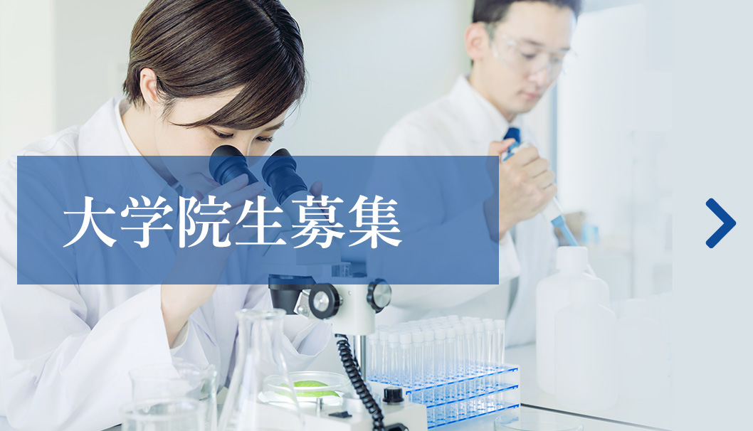
TOKYO UNIVERSITY OF SCIENCE
KOBAYASHI LAB
Sputtering for Materials Innovation
TOKYO UNIVERSITY OF SCIENCE
KOBAYASHI LAB
Sputtering for Materials Innovation
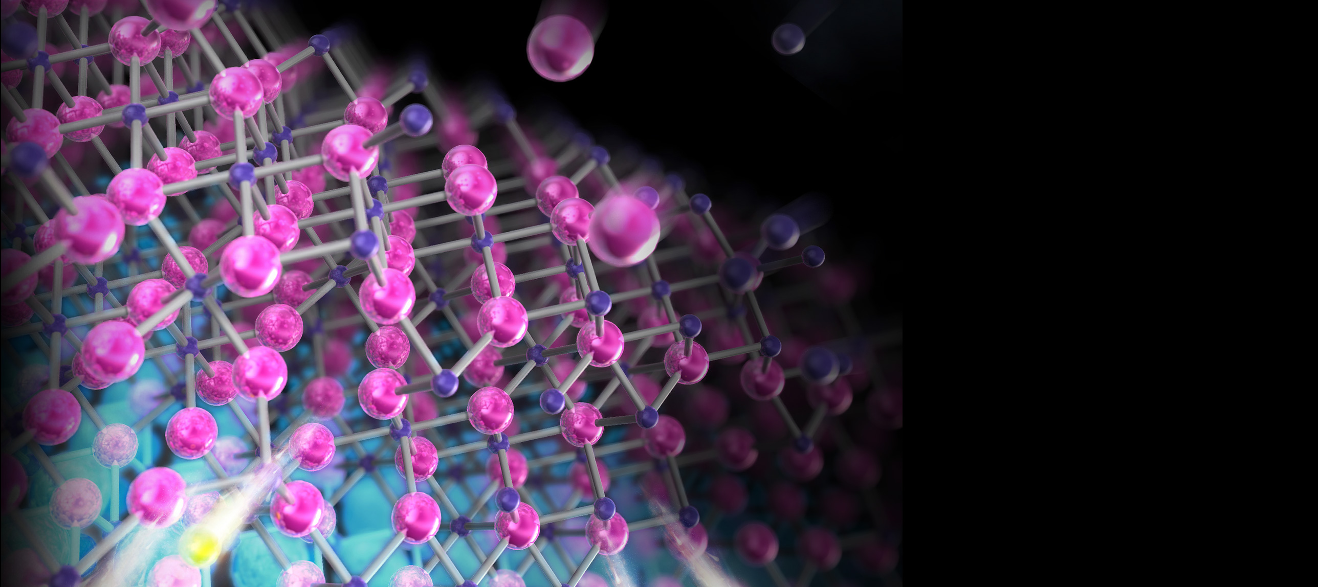
本研究室では、結晶成長によるマテリアルデザインを通じて、薄膜材料の機能融合に関する研究をおこなっています。 具体的には、半導体、超伝導体、強誘電体などの異種機能材料をナノスケールにまで薄膜化し互いに接合させることで、未来デバイス材料を創出することを目指しています。 特に、量子コンピュータ、量子情報通信、パワーエレクトロニクス、AI計算用新型半導体などの開発に繋がる薄膜材料の高品質化と高機能化に取り組んでいます。