TOKYO UNIVERSITY OF SCIENCE
KOBAYASHI LAB
Sputtering for Materials Innovation

TOKYO UNIVERSITY OF SCIENCE
KOBAYASHI LAB
Sputtering for Materials Innovation
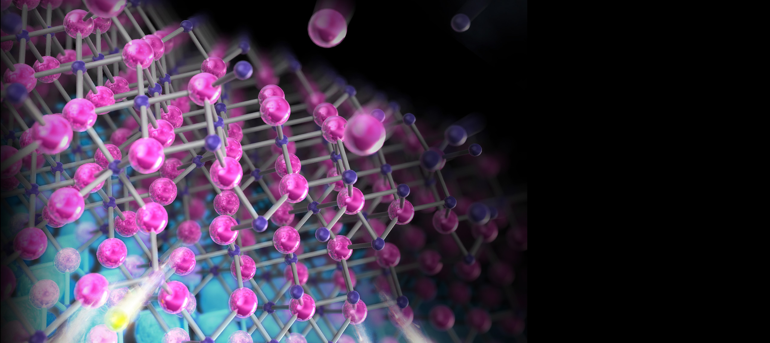
We study the integration of functional properties in thin-film materials through materials design based on crystal growth. By thinning dissimilar functional materials — semiconductors, superconductors, and ferroelectrics — down to the nanoscale and joining them together, we aim to create materials for future devices. In particular, we work on improving the crystalline quality and functionality of thin films that will enable quantum computing, quantum information technology, power electronics, and new semiconductors for AI computing.